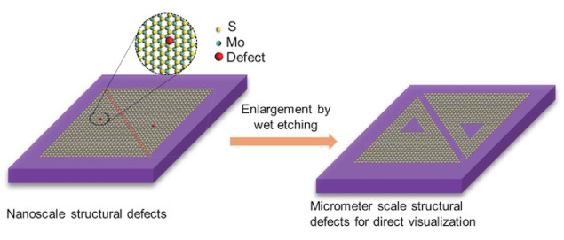
Directly visualizing structural defects in semiconductors on large scales is no easy task. The main microscopy techniques are limited to fields of view measuring just a few tens of nanometres, and they require ultrahigh vacuum, ultralow temperatures, complicated sample preparation and complex setups that make them impractical for many tasks. Now, researchers at the Chinese Academy of Sciences in Beijing have developed a simple and non-invasive alternative: a wet-etching technique that they claim could improve the performance of electronic devices by making it easier to understand their mechanical, electrical and optical properties.
Led by Guangyu Zhang of the Beijing National Laboratory for Condensed Matter Physics and the Songshan-Lake Materials Laboratory in Dongguan, the team developed the method as a simpler way of visualizing structural defects in a typical two-dimensional (2D) semiconductor, monolayer molybdenum disulphide (ML–MoS2). In the work, the researchers used a wet etching process that enlarged the structural defects in the semiconductor from nano- to micro-sizes, making the defects easier to observe under an optical microscope or atomic force microscope (AFM). The etching process involves applying a solution of 2% calcium hypochlorite by weight to the material for 20 seconds at room temperature, and because the defects are relatively reactive to chemical treatments, the process affects only the defected sites, leaving other areas of the ML–MoS2 lattice intact.
Triangular pits and trenches
After making the defects bigger, the researchers say they were able to observe 0D point defects (such as sulphur vacancies) and 1D grain boundaries that transformed into triangular pits and trenches, respectively, in different types of ML–MoS2. These were mechanically exfoliated MoS2, CVD-grown ML–MoS2, single domain and CVD-grown ML–MoS2 films with small and large grain size.
The number of triangular pits reached their maximum after roughly 200 seconds. According to Zhang and colleagues, this indicates that the etching process by hypochlorite ions initiates at inherent defect sites and does not generate new defects, unlike existing selective etching techniques. The increase in the number of pits over time may stem from the different chemical reactivity of different defects, they say.
General technique for directly visualizing defects
MoS2 belongs to a class of materials called 2D transition metal dichalcogenides (2D–TMDs), and the researchers say that their calcium hypochlorite solution can also be used to etch other materials of this type such as WSe2, MoSe2, and WS2. “This indicates that our method is a general technique for directly visualizing defects in 2D–TMDs and has the potential to be applied to other 2D semiconductors,” Zhang says.

First-principles calculations shed light on semiconductor defects
“Our simple and non-invasive method can directly visualize the structural defects in 2D–TMDs on a large scale,” he adds. Utilizing this etching technique, the team investigated the intrinsic defects of four types of ML–MoS2films and found that CVD-grown ML–MoS2single domain and ML–MoS2films with large grain size have lowest defect density. This enabled the researchers to understand the relationship between structural defects and performance.
“Being able to direct visualization of the structural defects in 2D semiconductors at a large scale in this way allows us to assess sample quality and could help guide us towards high-quality wafer growth,” he tells Physics World. It also makes it possible to identify relationships between the material’s structure and its performance, and thus to develop high-performance 2D devices towards practical applications, he adds.
Full details of the research are published in Chinese Physics B.