A new generation of CMOS image sensors now rivals the performance of state-of-the-art photon detectors for optical telescopes, while also operating at higher speeds and over a wider dynamic range
Ground-based astronomy remains at the forefront of our quest to understand more about the cosmos. While many celestial bodies in the night sky can be seen at visible wavelengths, the signal often becomes very faint by the time it reaches us here on Earth. Optical telescopes must therefore be equipped with light detectors that combine high sensitivity – converting as many incoming photons as possible into electrical measurements – with minimal noise.
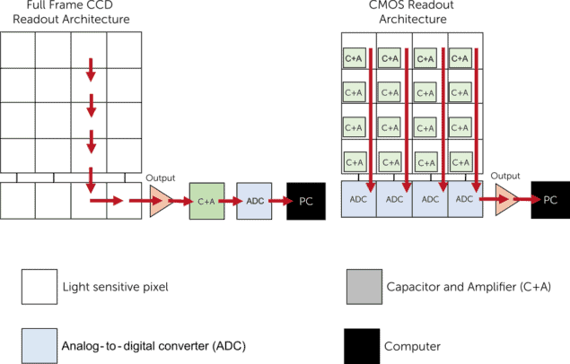
For decades the detector-of-choice has been the charge-coupled device (CCD), which combines a quantum efficiency of more than 95% in the visible with low-noise operation. An important advantage of CCDs is that they are back-illuminated, which means that the photodiodes used to convert the incoming photons into photoelectrons are positioned in front of the electrical circuitry. This maximizes the area available for photon capture, and also allows efficient cooling from the back of the sensor to reduce the build up of thermal noise during long exposures – which can last for several minutes or even longer.
However, CCDs have significant limitations at faster time scales, which are increasingly needed to observe dynamic processes or to enable quick analysis for applications such as adaptive optics. “A CCD usually only has a single read-out node,” explains Jason McClure, chief technology officer of Teledyne Princeton Instruments. “At the end of every exposure the photoelectrons generated in each pixel must be shifted across the sensor to reach the read-out node, and this slows down the read-out speed.”
Faster read-out times can be achieved by measuring the photoelectrons collected together at the end of each exposure with high-speed analogue-to-digital convertors (ADCs), but these can introduce high levels of read noise. Even at high ADC rates, long read-out times are a particular problem for large-area detectors with lots of pixels (4k x 4k or greater), ranging from seconds to dozens of seconds.
Another issue for the full-frame CCDs typically used in astronomy are the mechanical shutters that are used to block out incoming light during readout. These mechanical shutters have finite lifetimes and need frequent replacement when the camera is in heavy use – which can be problematic for remote observatories where maintenance can be challenging. Additionally, opening and closing a mechanical shutter is relatively slow, reducing the frame rate and generating quantitative errors for shorter exposure times.
Some of these issues have been addressed through the introduction of electron-multiplying CCDs (EMCCDs), which use on-chip amplification to boost the signal relative to the read noise. EMCCDs are able to detect much weaker signals than traditional CCDs, and can also operate at the higher frame rates needed to capture the evolution of dynamic events.
What’s more, many EMCCDs are equipped with electronic shutters that are faster and more precise than mechanical versions. “Electronic shutters also reduce the dead time during which the camera is unable to detect any incoming light,” adds McClure. “EMCCDs shift the detected photoelectrons into a frame storage area at the end of each exposure, which allows the next exposure to start while the signal is being read out from the storage area.”
Despite the advantages of EMCCDs, the random nature of the on-chip amplification process generates excess noise that limits the overall sensitivity when imaging brighter objects, typically when the signal is larger than a few photons per pixel. Their complex gain response can also make it more difficult to obtain reliable quantitative measurements, which has limited their use for some astronomical applications – as discussed in more detail in the article “Types of Camera Sensor“.
Alternative visions
While CCDs remain the most popular technology for ground-based astronomy, image sensors based on traditional CMOS technology now offer a viable alternative. “CMOS image sensors have not generally been suitable for astronomy because they are front illuminated, and are both less sensitive and more noisy than CCDs,” says McClure. “But more advanced CMOS imaging chips are now emerging that rival the performance of CCD and EMCCDs, while also overcoming the common limitations of these technologies.”
One of the big advances has been the introduction of back-illuminated CMOS sensors, which has increased the quantum efficiency to more than 90% in the visible range. Such CMOS designs are also more sensitive than a typical CCD at ultraviolet wavelengths, which makes them ideal for observations at multiple wavelengths.
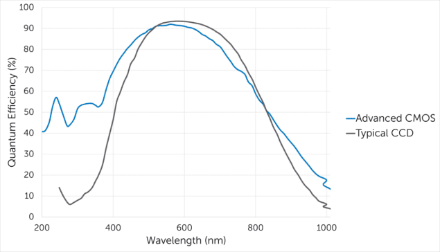
CMOS sensors are also able to process data at much higher speeds than CCDs, while maintaining low read noise and avoiding the excess random noise of EMCCDs. “CMOS designs have a parallel readout architecture,” explains McClure. “The charge-to-voltage conversion takes place at each individual pixel, allowing read-out nodes on every column of the sensor to operate simultaneously.”
Such high-speed operation makes CMOS designs ideal for large-area sensors, which allow more objects to be observed per frame for applications such as sky surveys. They also reduce the number of telescope movements needed to track rapidly moving objects, and enable improved image calibration by making it possible to record more reference stars.
According to McClure, CMOS cameras are now available with pixel counts of 6k x 6k and above, and with large pixel sizes of around 10 μm, to provide a large field of view. “They also offer high quantum efficiencies and low read noise for precise imaging of fainter, high-speed objects, or multiple fainter objects within one frame,” he adds.
CMOS imagers can also offer a wide dynamic range – which makes it possible to detect faint astronomical objects in the same field of view as brighter objects – without compromising on read-out speed. This is typically achieved by sampling the signal multiple times at high and low gain, but in many designs the high- and low-gain read-outs must be operated in different modes to keep the read noise down. This creates two different noise regimes, and when they are combined together artifacts emerge that often limit the precision of the measurements.
The solution in advanced CMOS designs, such as Teledyne Imaging’s LACera technology, is to improve the noise performance of the ADC. “Our patented dual ADC operates with very low read noise in high-gain mode, so we don’t have to crank up the gain to keep the read noise down,” explains McClure. “At this signal level our low-gain read-out is dominated by shot noise and you don’t see a stitching artifact at all.” The result, says McClure, is unsurpassed dynamic range at high frame rates, as described in more detail in Teledyne’s article “New Era in High Dynamic Range and Linearity for Scientific CMOS Cameras“.
CMOS sensors also have precise electronic shutters to enable continuous imaging without any loss of data. However, they typically exploit a rolling shutter – in which exposure and read-out progresses through the sensor one row at a time – instead of a global shutter, which reads and resets all the detector pixels at the same time. Although this rolling process is very fast, it can introduce distortions when imaging fast-moving objects as well as occasional delays between frames. Synchronization problems can also emerge that would be detrimental for many astronomy applications.
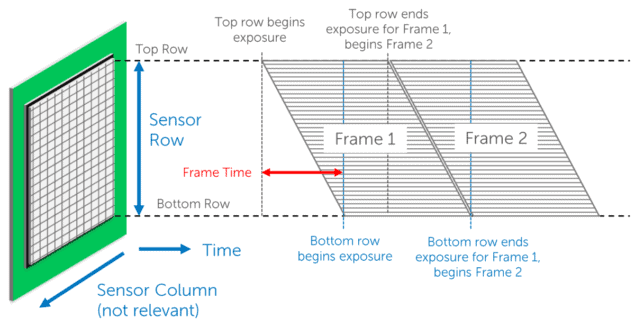
However, it has proved challenging to engineer a global shutter for back-illuminated CMOS sensors because this mode of operation requires all the photoelectrons to be moved into a storage area as soon as the exposure ends. This storage area is typically light-sensitive, which means that interactions with any stray photons can introduce artefacts into the image. For front-illuminated CMOS sensors the storage area can be hidden under the sensor components, but this is more difficult to achieve with back-illuminated designs.
Teledyne Imaging has solved this problem in its LACera technology by redesigning the storage area to minimize its sensitivity to light when the shutter is closed. Described in more detail in the company’s article “Achieving a True Global Shutter with Large Format, Back-Illuminated CMOS“, McClure says that the new design dramatically reduces the parasitic light sensitivity and enables true global shutter operation with minimal artifacts.
“Although CCD and EMCCD technologies have their advantages for ground-based astronomy, back-illuminated CMOS sensors match their performance while overcoming their limitations on speed, duty cycle and noise performance,” concludes McClure. “CMOS designs, with their combination of high quantum efficiency, high dynamic range, short readout times and low noise, offer a competitive alternative for a wide range of astronomy applications.”
