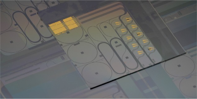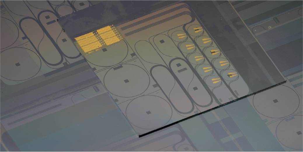
Researchers in the US have integrated ultralow-noise lasers and photonic waveguides onto a single chip for the first time. This long-sought-after achievement could make it possible to perform high-precision experiments with atomic clocks and other quantum technologies within a single integrated device, removing the need for room-sized optical tables in certain applications.
When electronics was in its infancy, researchers worked with diodes, transistors, and so on as stand-alone devices. The technology’s true potential was only realized after 1959, when the invention of the integrated circuit made it possible to pack all these components onto a chip. Photonics researchers would like to perform a similar feat of integration, but they face a hurdle: “For a photonic link we need to use a light source, which is normally a laser, as the transmitter to send the signal to the downstream optical links like the fibres or waveguides,” explains Chao Xiang, who led the research as a postdoc in John Bowers’ group at the University of California, Santa Barbara. “But when you send out the light, it will normally generate some back-reflection: that goes back into the laser and makes it very unstable.”
To avoid such reflections, researchers usually insert isolators. These allow light to pass in only one direction, breaking the natural two-way reciprocity of light propagation. The difficulty is that industry-standard isolators accomplish this using a magnetic field, which poses problems for chip-making facilities. “CMOS fabs have very strict requirements about what they can have in the clean room,” explains Xiang, who is now at the University of Hong Kong. “Magnetic materials are normally not permitted.”
Integrated, but separate
Since the high temperatures required for annealing waveguides can damage other components, Xiang, Bowers and colleagues began by fabricating ultralow-loss silicon nitride waveguides on a silicon substrate. They then covered the waveguides with several layers of silicon-based materials and mounted a low-noise indium phosphate laser at the top of the stack. Had they mounted the laser and the waveguide together, the etching involved in fabricating the laser would have damaged the waveguides, but bonding the subsequent layers on top sidestepped this problem.
Separating the laser and the waveguides also meant that the only way the two devices could interact was by coupling through an intermediate silicon nitride “redistribution layer” via their evanescent fields (the components of an electromagnetic field that do not propagate but instead decay exponentially away from a source). The distance between them thus minimized unwanted interference. “The top laser and the bottom ultralow-loss waveguide are very far away,” says Xiang, “so they can both have the best possible performance on their own. The control of the silicon nitride redistribution layer allows them to be coupled exactly where you want them to be. Without it, they would not couple.”
Combining the best active and passive devices
The researchers showed that this laser setup was robust to noise at the levels expected in standard experiments. They also demonstrated the usefulness of their device by producing a tuneable microwave frequency generator by adjusting the beat frequency between two such lasers – something not previously practical on an integrated circuit.
Given the enormous range of applications for ultralow-noise lasers in modern technology, the team say that being able to use such lasers in integrated silicon photonics is a big leap forward. “Finally, on the same chip, we can have the best active devices and the best passive devices together,” says Xiang. “For the next step, we are going to use those very ultralow-noise lasers to enable very complex optical functionalities like in, for example, precision metrology and sensing.”

Leaky-wave metasurfaces connect waveguides to free-space optics
Scott Diddams, an optical physicist at the University of Colorado, Boulder, US, who was not involved in the research, is impressed: “This problem of integrated lasers with optical isolators has been the bane of the community for at least a decade and no one had known how to solve the problem of making a really low-noise laser on chip…so this is a real breakthrough,” he says. “People like John Bowers had been working in this field for 20 years, and so they knew the basic building blocks, but figuring out how to make them all work perfectly together is not just like bolting pieces together.”
Diddams adds that the new integrated device is likely to be “very impactful” in quantum computing. “Serious companies are trying to build platforms that involve atoms and ions – those atoms and ions operate at very specific colours, and we talk to them with laser light,” he explains. “There is just no way that one is ever going to build a functioning quantum computer at scale without integrated photonics like this.”
The research is published in Nature.
