Two-qubit gates – the central building blocks of quantum computers – operate by exploiting tunnelling interactions between qubits. A team of researchers in Australia has now found a way to optimize these interactions in silicon by determining where the qubits should be positioned within the silicon crystal lattice. The work, which was carried out at the Centre of Excellence for Quantum Computation and Communication Technology (CQC2T) and Silicon Quantum Computing (SQC), is a step forward in the race to scale up silicon-based quantum processors.
Quantum tunnelling occurs when a particle passes through an energy barrier despite not having enough energy (according to classical physics) to overcome it. The phenomenon is at the heart of many modern technologies, including scanning tunnelling microscopy (STM), some types of CMOS electronics and quantum devices in which electrons are confined and manipulated.
Creating robust interactions between qubits
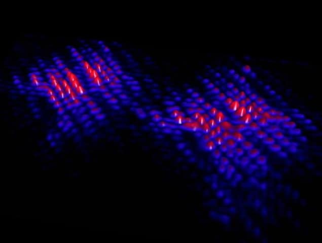
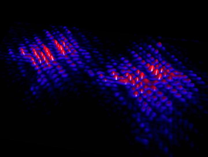
In 2018, the CQC2T/SQC team, led by Michelle Simmons of UNSW Sydney, used STM lithography to create qubits from phosphorus donor atoms in a silicon crystal. This technique makes it possible to position the atoms anywhere in a single atomic plane of the crystal. By placing phosphorus atoms a few nanometres from each other, the team created 2D donor arrays in which direct tunnelling interactions take precedence over dipolar (Coulomb) coupling. In this previous work, the researchers were able to map out the atoms’ wavefunction in 2D STM images and identify their exact spatial location.
In the new work, led this time by Sven Rogge, the researchers used STM to observe atomic-scale details of the interactions between coupled atom qubits. They also determined both the anisotropy in the wavefunction and the interference between the atoms directly in the plane. From this, the researchers learned that the positions of the qubits in the silicon lattice strongly affect the robustness of their interactions. In particular, they found that there is a special angle within the [110] plane of the silicon crystal in which these interactions are the most resilient. Such strong interactions are essential for making multi-qubit processors and, ultimately, a useful quantum computer.
Towards larger-scale processors
The advance in qubit positioning came about via a collaboration with researchers at the University of Melbourne. “Our colleagues at UNSW Sydney were able to obtain atomic-resolution images of coupled electron wave functions while we conducted advanced theoretical simulations to analyse these images and map the two-qubit interactions,” says CQC²T Deputy Director Lloyd Hollenberg, who led the Melbourne team. “We can use our previously-developed STM lithography technique to precisely place the phosphorus atoms at the special angle we discovered, so atom-based qubit devices could immediately benefit from the new result.”

Manufacturing silicon qubits at scale
The work, which is reported in Nature Communications, follows on from experiments done by the team in 2019 in which they used their precision placement approach to build the fastest two-qubit gate in silicon to date. The latest findings will allow for larger-scale processors, the researchers say.
The team is now working on building the first useful commercial quantum computer in silicon. “Since our results directly link to the STM lithography technique pioneered at UNSW, we hope to demonstrate enhanced device performance and reliability of multi-qubit devices fairly quickly,” study lead author Benoit Voisin tells Physics World. “We would also like to scale up our imaging technique to explore complex many-body regimes. For instance, strong tunnelling Coulomb couplings can be achieved at very short inter-dopant distances – a regime thought to be linked to high-temperature superconductivity.”
