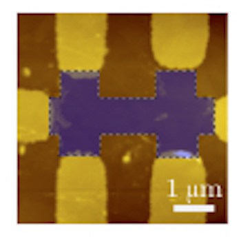
Researchers in China have observed a novel version of the Hall effect in a single layer of tungsten selenide (WSe2). The result, which they obtained by applying strain to a sample of the two-dimensional material, might aid the development of next-generation non-volatile magnetic memories.
The conventional Hall effect was first described in the late 19th century, and it occurs when electrons flow through a conductor in the presence of a magnetic field. The magnetic field exerts a sideways force on the electrons, leading to a voltage difference that is proportional to the strength of the field. More recently, scientists have uncovered a whole family of related effects, including the quantum, fractional and spin Hall effects.
In the nonlinear Hall effect, the voltage produced scales quadratically with the strength of the field, rather than linearly. This type of Hall effect, which was predicted theoretically in 2015, originates when a Hall current is generated in response to a “second-order” component of the electric field rather than a magnetic field. This second-order component is related to electrons’ orbital magnetism (that is, the magnetization induced by the particles’ orbital motion, rather than that caused by their spin), and it means that the charge carriers in a current travelling along a material can be deflected – thereby producing a Hall voltage – even without a magnetic field.
Few-layer TMDCs
In 2019, researchers observed the nonlinear Hall effect for the first time in few-layer tungsten ditelluride, WTe2, a material that belongs to the transition-metal dichalcogenide (TMDC) family of materials. Now, a team led by Zhi-Min Liao of the School of Physics at Peking University in Beijing, China, has found that the effect can also occur in a monolayer of a related TMDC, tungsten diselenide (WSe2), when the material is strained along its crystalline axis.
TMDCs have the chemical formula MX2, where M is a transition metal such as molybdenum or tungsten and X is a chalcogen such as sulphur, selenium or tellurium. In their bulk form, they act as indirect band-gap semiconductors, but when scaled down to a monolayer thickness, they behave as direct band-gap semiconductors, capable of efficiently absorbing and emitting light.
In the new work, reported in Chinese Physics Letters, Liao and colleagues studied flakes of WSe2 that they obtained by shaving off monolayer-thin slivers from bulk crystals of the material. To apply strain in the direction they wanted, they selected flakes with long, straight edges and transferred these onto a single crystal piezoelectric substrate known as PMN-PT. After they aligned the WSe2 flakes along the [001] orientation of the PMN-PT crystal, the used external electrodes to apply a voltage to the crystal along this same axis to generate a piezoelectric displacement and induce strain in the WSe2 flakes in this direction.

Collective electron excitations break down quantum Hall effect in graphene
Berry curvature dipole
By controlling the amount of strain applied, the researchers observed a quantum mechanical property known as a Berry curvature dipole, which dictates how moving charges (such as electrons) propagate through solid semiconductors. This Berry curvature dipole is directly related to the orbital magnetization in TMDCs when a current is applied to them. The researchers were therefore able to control this magnetization, which typically manifests itself perpendicular to the plane of the material, in a direct way by varying the external piezoelectric field.
Liao says that a similar tuning technique could be exploited in next-generation non-volatile magnetic memory devices using a phenomenon called orbit-magnetism torque (OMT). “Here, the information will be written by a charge current in a strained TMDC monolayer and the perpendicular magnetization switched by OMT,” he tells Physics World.
